This time, we will analyze the electric field of semiconductor devices using ELECTRIC-FIELD 3D (electric field analysis).
About electric field analysis in semiconductors
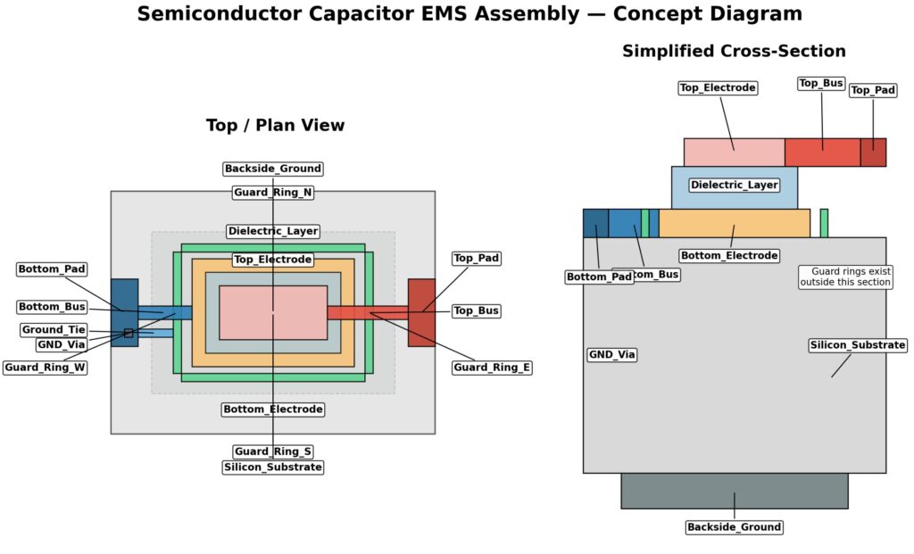
Figure 2: Conceptual diagram of a silicon capacitor
Inside semiconductors, electrons and holes are accelerated and moved by electric fields.
In other words, without understanding the electric field distribution, it is not possible to accurately grasp how current flows, how charge accumulates, where dielectric breakdown is likely to occur, or what the switching characteristics will be.
The main reasons are as follows.
1. To determine the movement of electrons and holes
Carriers in semiconductors move under electric fields, so by investigating the electric field distribution, we can predict current paths and charge transport behavior. This is especially important for MOSFETs, diodes, and IGBTs.
2. To prevent breakdown and leakage caused by high electric fields
If the electric field becomes too strong locally, it can cause dielectric breakdown, avalanche breakdown at pn junctions, increased tunneling current, and greater leakage.
Therefore, it is necessary to analyze where electric field concentration occurs.
3. To optimize device performance
The electric field distribution affects threshold voltage, on-resistance, breakdown voltage, switching speed, and parasitic capacitance.
Through analysis, electrode shape, doping distribution, insulating film thickness, and guard ring placement can be optimized.
4. Because problems become more evident as devices are miniaturized
As semiconductors become smaller, electric fields are more likely to concentrate in narrow regions.
Effects that could once be ignored become serious in fine devices, such as short-channel effects and hot-carrier degradation.
5. Because it is directly tied to breakdown voltage design in power semiconductors
In power devices such as SiC, IGBTs, and MOSFETs, the location of the maximum electric field determines breakdown voltage.
Electric field analysis is almost essential for designing termination structures and edge regions.
6. Because it can reduce the number of prototypes
Actually building and measuring devices takes time and cost.
Electric field analysis allows issues to be predicted before prototyping, making it easier to identify promising designs.
This time, we will analyze the electric field inside and around a capacitor, one of the most representative semiconductor components.
Electric field analysis of a silicon capacitor
We will perform electric field analysis of a silicon capacitor using ELECTRIC-FIELD 3D.
The analysis model is shown below.
Analysis model 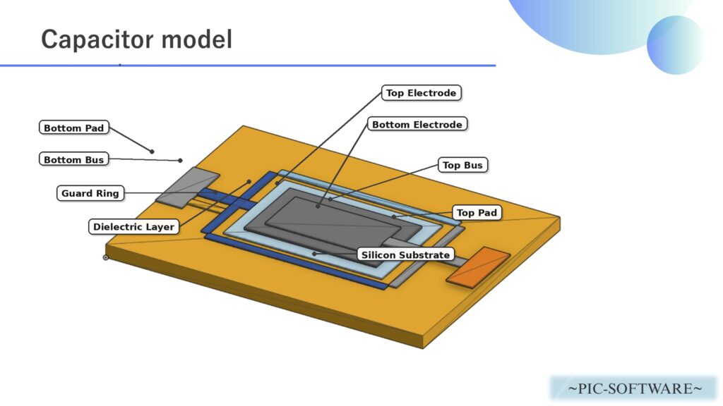
Figure 2: Analysis model of the silicon capacitor
We created an analysis model of the silicon capacitor as shown above and performed electric field distribution analysis inside the capacitor and in its surrounding area. The role of each component is as follows.
-
-
-
-
Top Pad
A terminal used to electrically connect to the upper electrode from the outside. It serves as the entry point for signals and voltage from measuring instruments or wiring. -
Top Bus
The wiring that connects the Top Pad and the Top Electrode. It is the conductor pattern that carries the potential to the upper electrode. -
Top Electrode
The upper electrode of the capacitor. It faces the Bottom Electrode to create the electric field and plays a major role in forming capacitance. -
Bottom Pad
A terminal used to connect to the lower electrode side from the outside. It is often used as the output terminal for the GND side or reference potential side. -
Bottom Bus
The wiring that connects the Bottom Pad and the Bottom Electrode. It carries the potential to the lower electrode. -
Bottom Electrode
The lower electrode of the capacitor. It forms the actual counter electrode paired with the Top Electrode and stores charge. -
Dielectric Layer
The insulating layer placed between the upper and lower electrodes. It blocks direct current flow while allowing the electric field to pass, enabling capacitor operation.
The thickness and relative permittivity of this layer greatly affect the capacitance value. -
Guard Ring
An auxiliary conductor placed around the main electrode. It is used to suppress fringe electric fields, leakage current, and parasitic capacitance effects at the edges, improving measurement stability and analysis accuracy. -
Silicon Substrate
The substrate material that supports the entire structure. In addition to being a mechanical support, it also affects parasitic capacitance and electric field distribution. For a semiconductor substrate, conductivity and permittivity settings strongly influence the analysis results.
-
-
-
Analysis conditions
The analysis conditions are shown below.
| Analysis software | PIC-PLASMA 3D or PIC-ELECTRON 3D or ELECTRIC-FIELD 3D |
| Analysis type | Electric field analysis |
| Analysis object | semiconductor.obj |
|---|
- Before
Model with insufficient electrode, GND, and material constant settings
| Component | Voltage | Relative permittivity εr |
|---|---|---|
| Top_Pad | +5 V | 1.0* |
| Top_Bus | +5 V | 1.0* |
| Top_Electrode | Not fixed | 1.0* |
| Bottom_Pad | 0 V | 1.0* |
| Bottom_Bus | 0 V | 1.0* |
| Bottom_Electrode | Not fixed | 1.0* |
| Guard_Ring_W/E/S/N | Not fixed | 1.0* |
| Ground_Tie | Not fixed | 1.0* |
| GND_Via | Not fixed | 1.0* |
| Backside_Ground | Not fixed | 1.0* |
| Dielectric_Layer | Not fixed | 1.0 |
| Silicon_Substrate | Fixed at 0 V | 1.0 |
- After
| Component | Voltage | Relative permittivity εr |
|---|---|---|
| Top_Pad | +5 V | 1.0* |
| Top_Bus | +5 V | 1.0* |
| Top_Electrode | +5 V | 1.0* |
| Bottom_Pad | 0 V | 1.0* |
| Bottom_Bus | 0 V | 1.0* |
| Bottom_Electrode | 0 V | 1.0* |
| Guard_Ring_W/E/S/N | 0 V | 1.0* |
| Ground_Tie | 0 V | 1.0* |
| GND_Via | 0 V | 1.0* |
| Backside_Ground | 0 V | 1.0* |
| Dielectric_Layer | Not fixed | 3.9 |
| Silicon_Substrate | Not fixed | 11.7 |

The figure below shows the input screen for the analysis conditions used this time in ELECTRIC-FIELD 3D.
Analysis Results
- Before
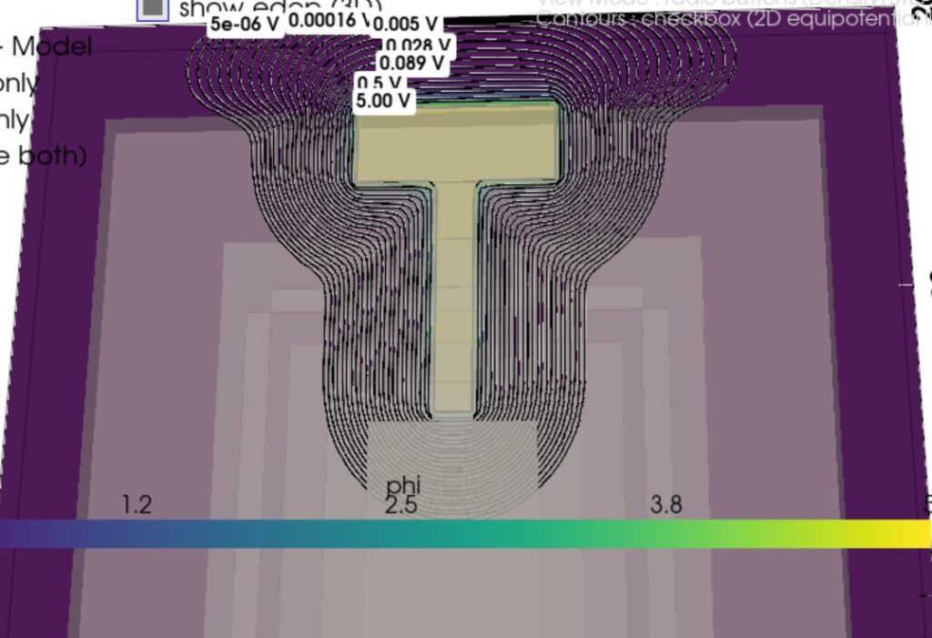 Cross section
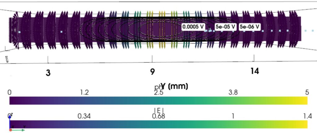
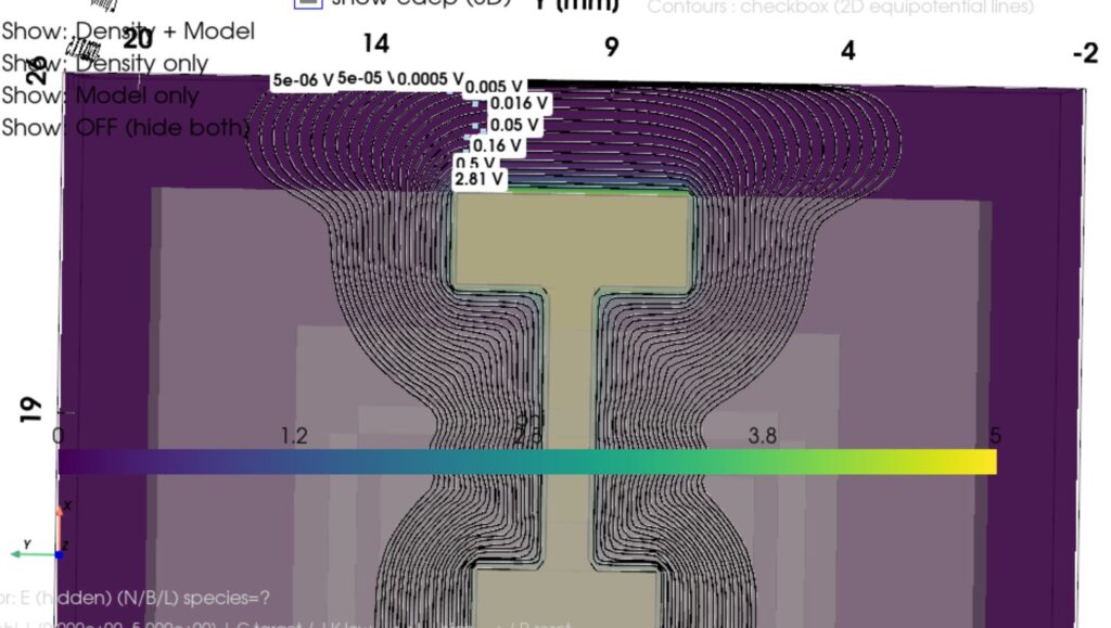
Figure 3: Electric field distribution of the model with insufficient electrode, GND, and material constant settings
- After
Overall
Cross section
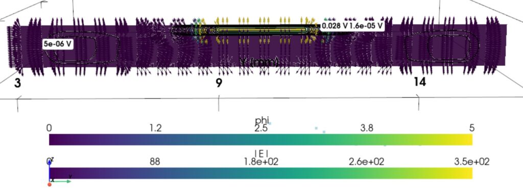 Figure 4: Model that properly reflects electrode potentials, grounding conditions, and material constants
The material above shows actual analysis results calculated with ELECTRIC-FIELD 3D.
Under the After condition, by properly setting the potential conditions of the main electrode, counter electrode, guard ring, and backside GND, the closure of the electric field became clear, and the unstable electric field distribution caused by floating conductors seen in the Before condition was resolved.
Please note that the CAD model used this time was created in a simplified manner, so electrode voltages and other condition settings have also been simplified.
*The above is just one example. Please make full use of the electric field analysis software ELECTRIC-FIELD 3D for your product development.*